
Raman Spectroscopy for Semiconductor Analysis
Raman Spectroscopy for Semiconductor Analysis
In modern semiconductor manufacturing and research, precision at the atomic and molecular level is not optional. It is foundational. As device geometries shrink and materials become more complex, characterization techniques must keep pace. Among the available analytical tools, Raman Spectrometer for Semiconductor analysis has emerged as a highly reliable, non-destructive method for probing structural, chemical, and electronic properties. This application note explains how Raman spectroscopy is applied in semiconductor analysis, what insights it provides, and where its limitations lie. It is written for engineers, researchers, and decision-makers who require both technical clarity and practical relevance. | 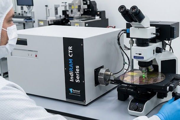 |
What is Raman Spectroscopy?
Raman spectroscopy is an optical technique based on the inelastic scattering of monochromatic light, typically from a laser source. When photons interact with a material, most scatter elastically (Rayleigh scattering), but a small fraction undergo energy shifts due to interactions with vibrational modes in the lattice. These shifts create a Raman spectrum, a molecular fingerprint of the material. For semiconductor materials, this fingerprint is directly tied to crystal structure, crystallinity, doping concentration, and layer thickness, strain, composition, and defects.
Why Use Raman Spectroscopy for Semiconductor Analysis?
The appeal of Raman Spectroscopy for Semiconductor applications comes down to a few key advantages:
Minimal sample preparation: Direct measurement on surfaces or through transparent layers
Non-destructive measurement: No need to damage or alter wafers
High spatial resolution: Especially with confocal systems
Sensitivity to lattice dynamics: Ideal for detecting strain and crystallinity
However, it’s worth questioning an implicit assumption: that Raman alone is sufficient for semiconductor characterization. In reality, Raman is powerful but not comprehensive. It is best used alongside techniques like XRD, SEM, or TEM when deeper structural or morphological insight is required.
Request a Custom Raman Spectroscopy Solutions »»
Applications in Semiconductor Analysis
1. Strain Measurement
Mechanical stress significantly impacts semiconductor performance, particularly in advanced nodes where strain engineering is deliberately introduced to enhance carrier mobility.
Raman spectrometer detects shifts in phonon frequencies, which correlate directly with strain. For example:
Tensile strain typically causes a downward shift (Red Shift) in Raman peaks
Compressive strain causes an upward shift (Blue shift)
This makes Raman a preferred tool for mapping strain distributions across wafers and devices.
Critical perspective: While Raman provides relative strain measurements with high spatial resolution, absolute quantification depends heavily on calibration models, which may vary between materials and device structures.
2. Material Identification and Composition Analysis
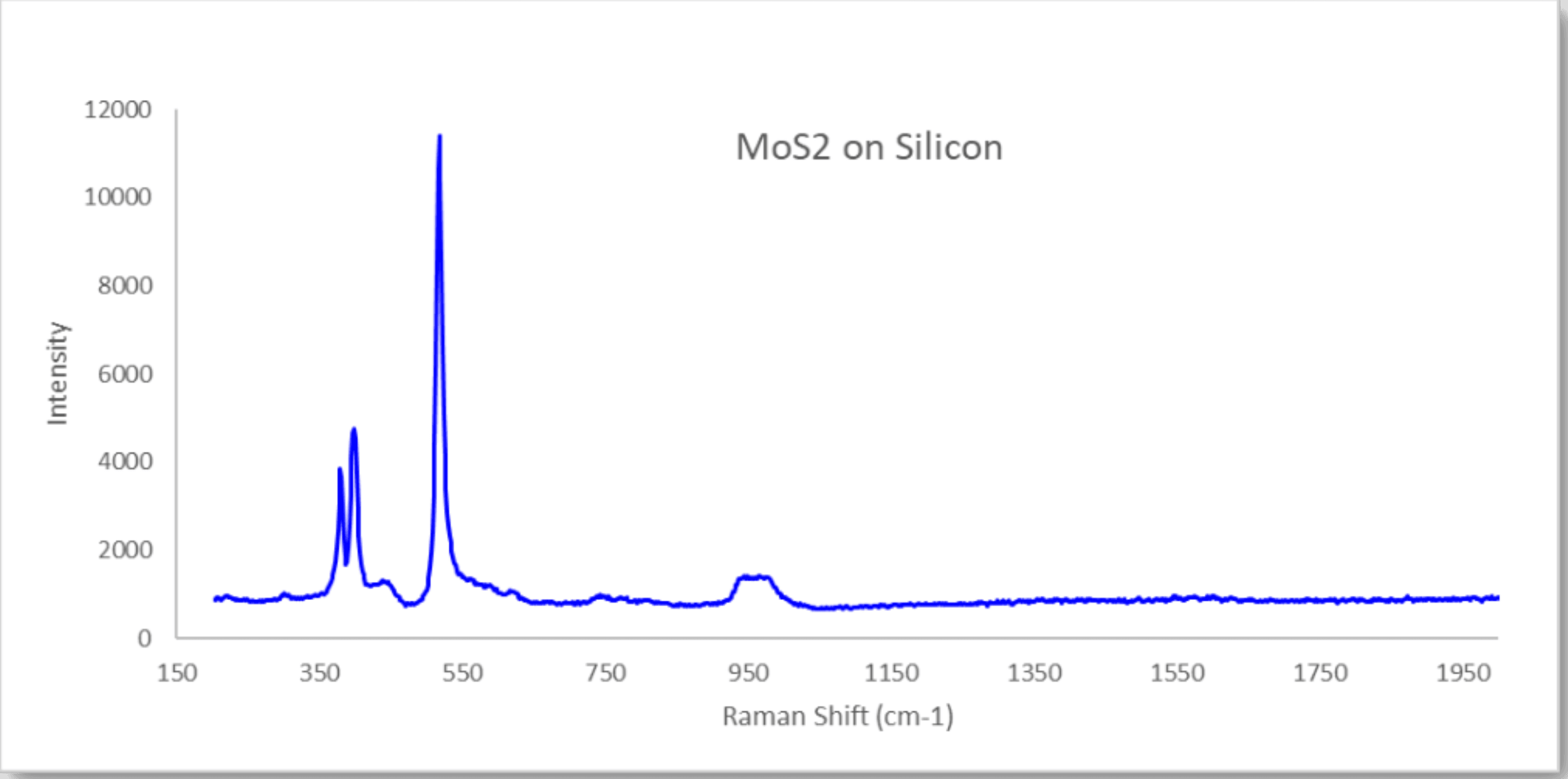
Semiconductors often involve compound materials such as SiGe, GaN, or III-V alloys. Raman spectroscopy distinguishes these based on characteristic vibrational modes.
Identifies phase composition.
Detects alloy ratios (e.g., Ge content in SiGe).
Differentiates crystalline vs. amorphous regions.
Skeptical note: Overlapping Raman peaks in complex alloys can complicate interpretation. Without proper spectral deconvolution or reference standards, misidentification is possible.
3. Defect and Crystal Quality Analysis
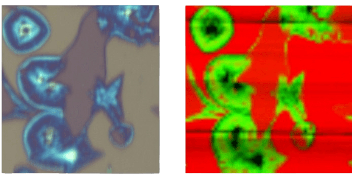
Crystal defects, dislocations, and amorphous regions alter the Raman signal:
Peak broadening indicates disorder
Reduced intensity suggests poor crystallinity
Additional peaks may indicate defect-related modes
This makes Raman useful for quality control during epitaxial growth or post-processing.
Alternative view: Raman is sensitive to lattice disorder, but it cannot always distinguish between different defect types. Complementary methods are often needed for precise defect classification.
 |  |
4. Thin Film and Layer Characterization
With confocal Raman Spectroscopy systems, depth profiling becomes possible:
- Measures thickness of thin films
- Identifies multilayer structures
- Analyzes interfaces in stacked devices
This is particularly useful in advanced packaging and 3D semiconductor architectures.
5. Process Monitoring and Inline Inspection
Raman spectroscopy is increasingly integrated into semiconductor production lines:
- Real-time monitoring of stress and composition
- Rapid wafer mapping
- Detection of process-induced variations/defects
Because it is non-contact and fast, it fits well into high-throughput environments.
Raman Spectroscopy Instrumentation
A typical Raman system for semiconductor analysis includes:
- Laser source (commonly 320nm, 488nm, 514.5nm 532 nm, 633 nm, or 785 nm)
- Optical microscope for focusing
- Spectrometer with high spectral resolution
- Sensitive detector (CCD)
Choice of wavelength affects penetration depth and signal strength, so it must align with the material system.
Conclusion - Raman Spectroscopy for Semiconductor analysis provides a powerful, non-destructive way to probe material properties at the microscopic level. Its strengths lie in detecting strain, identifying materials, and assessing crystal quality with high spatial resolution. At the same time, its effectiveness depends on careful interpretation, proper calibration, and integration with complementary techniques. Used thoughtfully, Raman spectroscopy is not just a diagnostic tool - it is a strategic asset in semiconductor research and manufacturing.
Request for Information
Do you have any questions or requests? Use this form to contact our team.